In 30 Sekunden
Apple reuses a CPU die with two sizes of GPU die across the M5 Pro and Max, while the Ultra combines two CPU and two large GPU dies. SemiAnalysis and its STEEL lab found that the chips use hybrid bonding to connect side-by-side dies through a silicon interposer, replacing solder bumps with direct copper contacts. The presenter expects the smaller connections to improve bandwidth and energy efficiency. The Ultra’s own interconnect remains an inference from the Max die and Apple’s published density claim: the lab had not yet examined an Ultra.
- 1The new dies divide functions rather than joining two complete chipsThe presenter distinguishes the new design from previous Ultra packages that joined two fully functional Max dies.
- 2One CPU die pairs with either of two GPU sizesM5 Pro combines the CPU and smaller GPU; Max uses the larger GPU, while Ultra joins two of each larger configuration.
- 3The smaller GPU has half the cores, cache and memory widthThe larger die has 40 GPU cores, 48 MB system cache and a 512-bit interface; the smaller has 20, 24 MB and 256 bits.
- 4Hybrid bonding connects neighboring dies without solder bumpsApple uses TSMC’s face-to-face process to bond chiplets to a silicon interposer through directly connected copper contacts.
- 5A second interface suggests how the Ultra joins two Max assembliesThe lab had not obtained an Ultra. It infers the packaging from the Max’s second interface and Apple’s stated increase in connection density.
Das Wichtigste
- The M5 Pro and Max share a CPU die but pair it with different GPU dies.
- Hybrid bonding can fit more contacts into a given area than conventional solder microbumps.
- The presenter infers that the Ultra also uses hybrid bonding, but the lab had not yet inspected that chip.
- The small GPU die has half the large die’s cores, system cache and memory-interface width.
Den bearbeiteten Text nach Kapiteln lesen
Why the M5 changes the chiplet arrangement
The presenter distinguishes joining complete Max chips from dividing CPU and GPU functions across dies. Apple combines three die designs into the Pro, Max and Ultra.
The M5 Pro, Max and Ultra share silicon as well as an architecture. I call this Apple’s first true chiplet design: the company has joined dies in earlier Ultra chips, but this generation divides functions across different dies. SemiAnalysis bought the chips and our STEEL lab took them apart to examine the packaging.
Earlier Ultra designs joined two complete Max chips. Each Max die could already function on its own. My distinction is that a chiplet design aims to optimize the area of individual dies for yield and moves different parts of the system onto separate dies that work together.
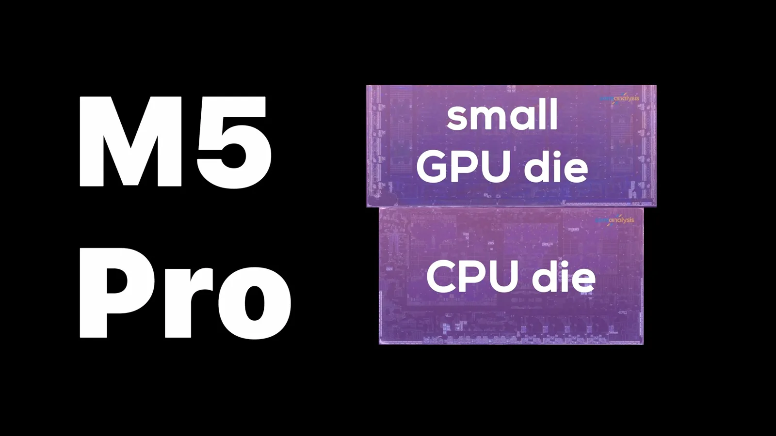
Apple made three die designs: one CPU and two GPU sizes. The Pro pairs the CPU die with the smaller GPU; the Max pairs it with the larger one. The Ultra combines two CPU dies and two large GPU dies.
Inside the shared CPU die
The die contains 18 CPU cores and shared caches, plus a neural engine, display and external interfaces. The presenter highlights the area occupied by high-speed I/O.
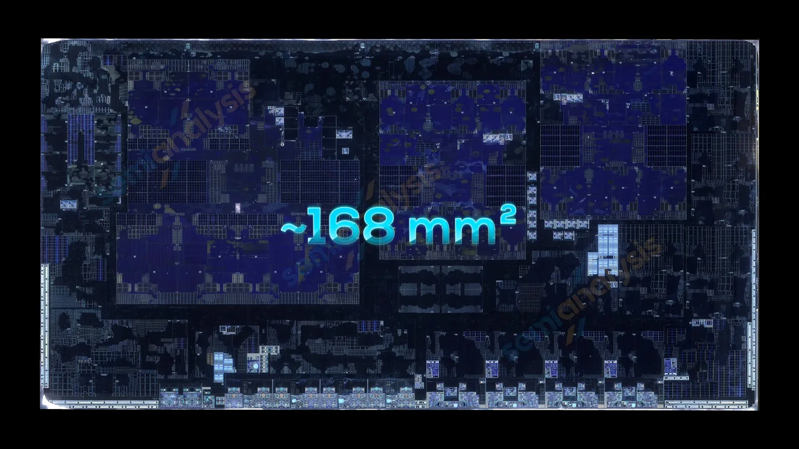
The shared CPU die is made on TSMC’s N3P process and measures about 168 square millimeters. It has 18 CPU cores in three clusters: six S-cores around a shared 16 MB cache, and 12 newer P-cores, internally called M-cores, split into two mirrored groups of six.
Each S-core has a private 1 MB L2 cache slice. Each six-core M cluster has 8 MB of shared cache, and each cluster has a dedicated AMX unit. The split may allow an entire cluster to be shut down for power management; there are no E-cores on this CPU die.
A 16-core Apple Neural Engine sits to the left of the M-cores. The Ultra doubles that neural processing capacity because it has two CPU dies. Four display engines and a row of input and output interfaces occupy other parts of the die.
The I/O includes interfaces for cameras and sensors, a four-lane display interface and 16 PCI Express lanes that appear likely to be generation 5. Four Thunderbolt 5 physical interfaces take up substantial silicon area, as do their control circuits. The die also contains a NAND controller and an AES engine in the secure enclave.
Along the upper edge is a long striped structure: the physical layer of the connection to another die. To understand why that connection matters, first look at the two GPU dies.
Two GPU dies share a family resemblance
The large GPU die has roughly twice the area and twice several resources of the smaller die. Both present matching interfaces for the CPU connection.
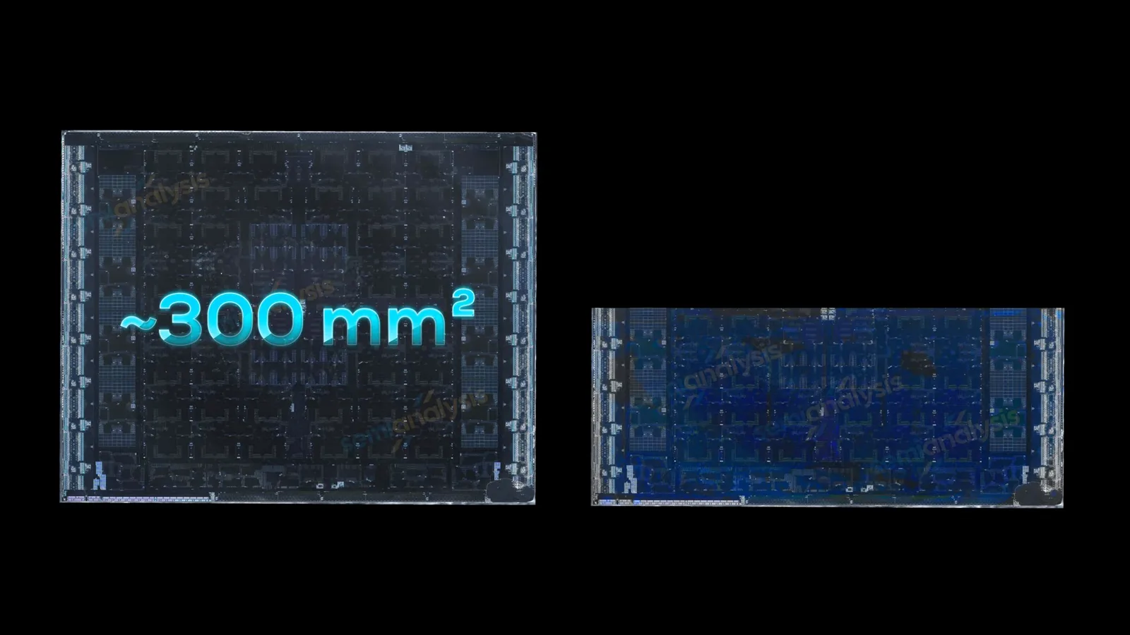
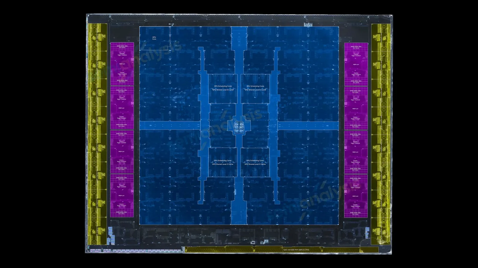
Both GPU dies use N3P. The large die measures about 300 square millimeters and the small one about 157. The large GPU has 40 cores, 48 MB of system-level cache and a 512-bit memory interface; the smaller die has half of each. Some media acceleration logic near the interface remains the same.
Placed as they are in the package, the CPU and GPU dies have matching physical interfaces along adjacent edges. Apple uses TSMC’s SoIC-mH, which TSMC also calls SoIC-X face-to-face, to connect them.
Hybrid bonding links dies through an interposer
TSMC’s face-to-face process places the dies beside one another. Direct copper contacts can be finer than solder bumps, increasing connection density.
Hybrid bonding has been used to stack a cache die on a compute die. Here the chiplets are side by side and bonded to a specially prepared silicon interposer. The “mH” name refers to molding them horizontally.
A conventional interposer connection uses microbumps: tiny solder contacts between finished dies and the interposer. Their size limits how densely the connections can be packed, and data moving between dies must pass through them.
Hybrid bonding instead aligns exposed copper contacts surrounded by insulating material on the dies and interposer. Heating expands and joins the copper directly. The presenter says solder microbumps are around a 25-micrometer pitch, potentially falling to 18, whereas hybrid bonding can go below 10 and approach 3 micrometers in advanced processes.
Denser connections offer the potential for high bandwidth, low latency and more energy-efficient transfers. Placing the dies beside one another rather than stacking them also avoids the thermal issues associated with that stack, the presenter argues.
Inferring the Ultra’s larger connection
The lab had not inspected an Ultra, but the large GPU die has a second interface. Apple’s density claim leads the presenter to infer hybrid bonding there as well.
The lab had not obtained an M5 Ultra. On the large GPU die of the Max, however, there is a second, larger interface opposite the CPU connection. Its similar structure suggests another hybrid-bonded link.
Apple says UltraFusion connects two dual-die Max assemblies and raises connection density by more than six times. The earlier M3 Ultra used a local silicon interconnect with solder microbumps measured at roughly 25 micrometers. The presenter calculates that the new density implies a pitch of about 10 micrometers or less and infers hybrid bonding.
The presenter sees the side-by-side arrangement as consistent with Apple’s attention to thermals and speculates that Apple may have worked with TSMC on the implementation. Direct copper contacts and higher density, in this analysis, reduce the energy needed to move data and increase potential bandwidth.
Mehr aus diesem Kanal
 51:27EN
 SemiAnalysis· 13. Nov. 2026Podcast · 3 StimmenNVIDIA’s CEO transition puts China chip policy and execution in focusGast: Jordan Schneider · Moderation: Jordan Nanos, Dylan PatelThe hosts debate chipmaking controls, cloud access and whether NVIDIA can retain its execution edge after Jensen Huang’s exit.
 42:39ENSemiAnalysis· 4. Nov. 2026Podcast · 4 StimmenHow the Midterms Could Reshape the 2028 Data Center BuildoutGast: Maya Barkin, Wayne Ma, Jeremie Eliahou Ontiveros · Moderation: Jordan NanosSemiAnalysis examines permitting, grid costs and the local backlash behind a more uncertain US data center pipeline.
 51:52ENSemiAnalysis· 3. Nov. 2026Podcast · 3 StimmenHow GDPx Tests Frontier AI: Inside SemiAnalysis’s New BenchmarkGast: Max Kan, Andrew Megalaa · Moderation: Jordan NanosThe team behind GDPx explains task quality, domain selection, grading and the trade-off between public scrutiny and private evaluations.
 55:06ENSemiAnalysis· 27. Okt. 2026Podcast · 4 StimmenAnthropic's S-1: Revenue, Compute Costs and the Race to ScaleThe SemiAnalysis panel examines Anthropic’s filing, from improving compute economics to customer concentration and competition.
 34:35ENSemiAnalysis· 23. Okt. 2026Podcast · 3 StimmenSemiAnalysis on ASML's Hybrid-Bonding Patents, HBM Economics and the Next Tool EcosystemGast: Sherry Zhang, Howie · Moderation: Jordan NanosJordan Nanos, Sherry Zhang and Howie examine a track-based bonding design that brings the wafer to the die, then explain why adoption depends on precision, cleanliness, economics and a changing supply chain.
 34:47ENSemiAnalysis· 20. Okt. 2026Podcast · 3 StimmenWhy SemiAnalysis Raised Its 2027 Data Center ForecastGast: Jeremie Ontiveros, Reyk Knuhtsen · Moderation: Jordan NanosJeremie Ontiveros and Reyk Knuhtsen explain their project-level model, construction risks and the possibility of a future capacity imbalance.