30초 요약
At the Silicon Valley 101 Alignment 2026 event, Duke assistant professor Harry Wang explains why shrinking silicon is difficult and why two-dimensional semiconductors face manufacturing and yield challenges. He describes his lab’s AI-assisted microscopy, experiments with Google DeepMind, and an unpublished small-scale fabrication demonstration, then offers a speculative vision of models and chips co-evolving.
- 1Why thin materials matterWang uses leakage and gate control to explain interest in thin semiconductor channels.
- 2Yield is the manufacturing hurdlePromising individual devices must be made reliably across a large number of transistors.
- 3AI-controlled microscopyATOMIC combines instrument control, segmentation, and clustering to inspect materials.
- 4Experiments in the physical worldA collaboration with Google DeepMind connects scientific planning with laboratory instruments, while retaining human steps.
- 5An unpublished fabrication prototypeWang describes selecting good locations on imperfect material for a small transistor array.
- 6A speculative feedback loopHe proposes “autogenic intelligence” as a name for AI and chips potentially co-evolving.
핵심 정리
- Two-dimensional semiconductors can be extremely thin, but producing uniform material at scale remains difficult.
- Wang describes microscopy workflows that use AI to inspect and classify material and defects.
- A lab collaboration uses AI to propose experiments and interact with instruments, while people still perform some physical steps.
- Wang presents an unpublished prototype that selects fabrication sites on imperfect material; it is not a production-scale chip.
- The proposed feedback loop between AI and chip manufacturing is a vision for future work, not an achieved autonomous system.
챕터별로 다듬은 전문 읽기
The AI–chip loop and semiconductor basics
Wang introduces transistors, scaling, and the link between AI and chip development.
I want to explain how chips are made from raw materials, what might come after silicon, and how my lab is using AI to accelerate semiconductor discovery and manufacturing. My central idea is a feedback loop: AI needs chips, and chip development can increasingly use AI.

I will start with semiconductor basics. Even sophisticated computing ultimately relies on binary states. The transistor acts like a faucet: a gate controls whether electrons flow between source and drain, allowing a circuit to represent on and off.
Putting more transistors into a chip can increase what it can do. As an illustration, I cite an AI processor with hundreds of billions of transistors. The historical question is how to fit so many switches into a limited footprint.
The industry has reduced transistor dimensions from micrometer to nanometer scales and moved from planar designs to FinFET and stacked nanosheets. But stacking introduces issues including heat at interfaces, while shrinking makes leakage and control harder.
Beyond silicon
He discusses leakage, ultrathin materials, and the difference between nominal nodes and physical dimensions.
In my faucet analogy, leakage is current finding a path even when the gate is off. A thinner channel can improve control: ideally the off state blocks flow, while the on state allows electrons through. This is part of the motivation for very thin semiconductor materials.
I argue that silicon becomes difficult to shrink indefinitely: at very small thicknesses, carrier mobility degrades. Two-dimensional materials, including molybdenum disulfide, are being studied because they can retain useful electronic properties at extremely small thicknesses.
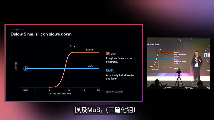
You may ask why chipmakers advertise two- or one-nanometer nodes if I discuss a physical silicon limit. Modern node names are nominal labels, not a direct measurement of every feature. Stacked structures also let engineers increase density without simply shrinking one element indefinitely.
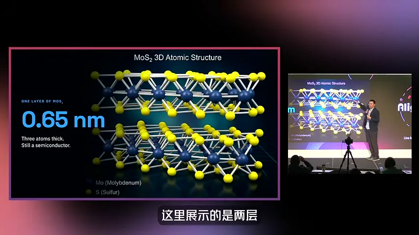
A single layer of molybdenum disulfide is about 0.65 nanometers thick. Research has shown promising individual devices made with such materials, but a successful laboratory transistor is not yet the same thing as a manufacturable chip.
Materials and manufacturing yield
He describes material growth, wafer-scale quality, and why yield is a central hurdle.

I show a TSMC roadmap moving from nanosheets toward CFET and, potentially, two-dimensional transition-metal dichalcogenides. The challenge is building these materials reliably across the enormous number of transistors needed on a chip.
One laboratory method is chemical vapor deposition: gaseous precursors react to grow an extremely thin semiconductor on a substrate. The material can work as a transistor channel, but achieving silicon-like uniformity and purity at wafer scale is difficult.
The practical issue is yield. A chip may contain vast numbers of transistors, and manufacturing needs them to work reliably. I argue that new two-dimensional semiconductors need approaches to yield management suited to their defects and fabrication process.
AI-assisted microscopy
His lab uses instrument control and image analysis to inspect materials and identify defects.
Traditionally, people inspect materials and defects as part of this process. About two years before the talk, my lab began asking whether AI could help see and classify these small structures, using microscopy as a starting point.
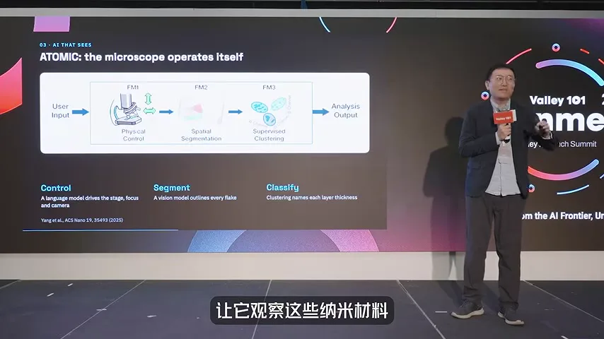
We call the published workflow ATOMIC. A language model helps control the microscope; image segmentation and clustering then identify features in the captured images. The goal is to distinguish useful material, defects, bare substrate, and other regions.
I say the system can identify single-layer and multilayer material and classify what it sees. The slide reports 99.7% pixel-level accuracy for monolayer MoS₂ and about six seconds per field of view; I note that latency remains a problem and that we are working to reduce it.

In one example, a human labels the visible flakes, while the model can also identify domain boundaries that matter as defects. I attribute part of the difference to pixel-level analysis, and emphasize that this is a result for particular tasks, not every scientific judgment.
We also tried other materials, including graphene and other two-dimensional semiconductors. I describe using a general system with prompts rather than training a new model for each material in these experiments.
AI-designed experiments
He explains a collaboration that connects scientific planning to instruments and retains human steps.
Seeing materials is only part of the problem: researchers must also make them. I expect AI for engineering to become increasingly important alongside AI for science, especially when ideas have to be tested in physical experiments.
My lab collaborated with Google DeepMind to extend a co-scientist approach into physical experiments. The system can review literature, propose ideas, produce experimental plans, and interact with a laboratory setup to test them.
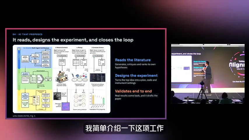
The workflow is not fully autonomous today. In the demonstration, people still weigh precursors, place them in a tube, and seal it. I suggest a robotic arm could eventually help with those physical steps, but that is a future possibility.
The system produced experimental recipes for known two-dimensional materials, and our paper explores the possibility of growing theoretically predicted materials that have not yet been made. I present that latter possibility as a research direction, not a demonstrated universal capability.
Reproducibility is hard because laboratories use different furnaces, tubes, and geometries. I describe giving the AI the local setup and asking it to adapt a published recipe to those instruments, with encouraging results in our experiments.
I recall asking students to grow two materials and then trying a language-model-generated recipe. In that example the recipe worked, which I say saved time. It is a lab anecdote, not evidence that generated recipes will always work on a first attempt.
From materials to prototype chips
He describes an unpublished small-scale fabrication result and potential commercial directions.
The next question is whether AI can help build a chip rather than only inspect or grow material. I show work that I say was not yet published: the microscope examines deliberately imperfect material and the system selects better areas for transistor fabrication.

Instead of assuming every location is equally suitable, the process adapts to local defects. I say the prototype connects AI with cleanroom instruments and produces arrays with thousands of transistors. It is a small-scale starting point rather than a production-scale chip.

The slide reports device yield rising from 65.6% to 94.4% with the prototype, an increase of 28.8 percentage points. I regard this as promising, while noting that the result shown was not yet published and the transistor array is far smaller than an industrial chip.
I mention a recently formed startup and plans around yield intelligence, lab-to-fab tools, and a possible pilot line for two-dimensional semiconductors. These are proposed commercial directions, not evidence that the approach is already deployed at industrial scale.
A vision of co-evolving intelligence
Wang proposes a speculative feedback loop between models and chip manufacturing, and asks whether systems might converge.
The longer-term idea is a flywheel: AI helps design and manufacture chips, and the resulting chips run and train AI. I call a possible future form of that closed loop “autogenic intelligence.” It is a conceptual proposal, not an achieved autonomous system.
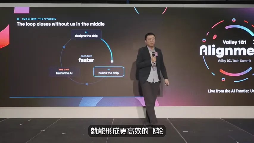
I compare the proposed integration of models and hardware with the relationship between mind and brain, and speculate about a possible new form of intelligence. The analogy is intended to provoke questions about co-evolution, not to establish that a chip-and-model system is alive.
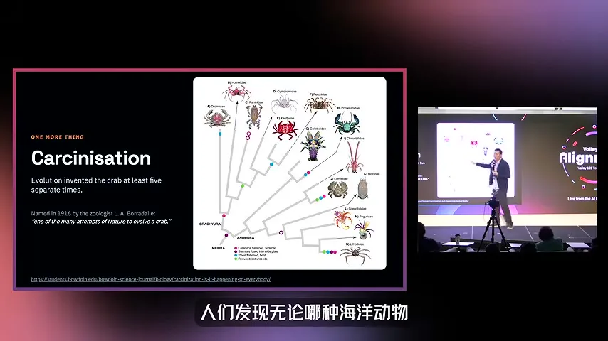
I end by asking whether such systems would diversify or converge on similar forms, using carcinization as a provocative analogy. This is an open question about a speculative future, not a biological proof that unrelated animals all become crabs.